50 Speakers Featured at the 2023 SNIA Compute+Memory+Storage Summit

SNIA CMS Community

Apr 3, 2023

title of post
SNIA’s Compute+Memory+Storage Summit is where architectures, solutions, and community come together. Our 2023 Summit – taking place virtually on April 11-12, 2023 – is the best example to date, featuring a stellar lineup of 50 speakers in 40 sessions covering topics including computational storage real-world applications, the future of memory, critical storage security issues, and the latest on SSD form factors, CXL™, and UCIe™. “We’re excited to welcome executives, architects, developers, implementers, and users to our 11th annual Summit,” said David McIntyre, C+M+S Summit Co-Chair, and member of the SNIA Board of Directors.  “We’ve gathered the technology leaders to bring us the latest developments in compute, memory, storage, and security in our free online event.  We hope you will watch live to ask questions of our experts as they present, and check out those sessions you miss on-demand.” Memory sessions begin with Watch Out – Memory’s Changing! where Jim Handy and Tom Coughlin will discuss the memory technologies vying for the designer’s attention, with CXL™ and UCIe™ poised to completely change the rules. Speakers will also cover thinking memory, optimizing memory using simulations, providing capacity and TCO to applications using software memory tiering, and fabric attached memory. Compute sessions include Steven Yuan of StorageX discussing the Efficiency of Data Centric Computing, and presentations on the computational storage and compute market, big-disk computational storage arrays for data analytics, NVMe as a cloud interface, improving storage systems for simulation science with computational storage, and updates on SNIA and NVM Express work on computational storage standards. CXL and UCIe will be featured with presentations on CXL 3.0 and Universal Compute Interface Express™ On-Package Innovation Slot for Compute, Memory, and Storage Applications. The Summit will also dive into security with a introductory view of today’s storage security landscape and additional sessions on zero trust architecture, storage sanitization, encryption, and cyber recovery and resilience. For 2023, the Summit is delighted to present three panels – one on Exploring the Compute Express Link™ (CXL™) Device Ecosystem and Usage Models moderated by Kurtis Bowman of the CXL Consortium, one on Persistent Memory Trends moderated by Dave Eggleston of Microchip, and one on Form Factor Updates, moderated by Cameron Brett of the SNIA SSD Special Interest Group. We will also feature the popular SNIA Birds-of-a-Feather sessions. On Tuesday April 11 at 4:00 pm PDT/7:00 pm EDT, you can join to discuss the latest compute, memory, and storage developments, and on Wednesday April at 3:00 pm PDT/6:00 pm EDT, we’ll be talking about memory advances. Learn more in our Summit preview video, check out the agenda, and register for free to access our Summit platform! The post 50 Speakers Featured at the 2023 SNIA Compute+Memory+Storage Summit first appeared on SNIA Compute, Memory and Storage Blog.

Olivia Rhye

Product Manager, SNIA

Leave a Reply

Comments

Name

Email Adress

Website

Save my name, email, and website in this browser for the next time I comment.

“Year of the Summit” Kicks Off with Live and Virtual Events

SNIA CMS Community

Mar 24, 2023

title of post
For 11 years, SNIA Compute, Memory and Storage Initiative (CMSI) has presented a Summit featuring industry leaders speaking on the key topics of the day.  In the early years, it was persistent memory-focused, educating audiences on the benefits and uses of persistent memory.  In 2020 it expanded to a Persistent Memory+Computational Storage Summit, examining that new technology, its architecture, and use cases. Now in 2023, the Summit is expanding again to focus on compute, memory, and storage. In fact, we’re calling 2023 the Year of the Summit – a year to get back to meeting in person and offering a variety of ways to listen to leaders, learn about technology, and network to discuss innovations, challenges, solutions, and futures. We’re delighted that our first event of the Year of the Summit is a networking event at MemCon, taking place March 28-29 at the Computer History Museum in Mountain View CA. At MemCon, SNIA CMSI member and IEEE President elect Tom Coughlin of Coughlin Associates will moderate a panel discussion on Compute, Memory, and Storage Technology Trends for the Application Developer.  Panel members Debendra Das Sharma of Intel and the CXL™ Consortium, David McIntyre of Samsung and the SNIA Board of Directors, Arthur Sainio of SMART Modular and the SNIA Persistent Memory Special Interest Group, and Arvind Jaganath of VMware and SNIA CMSI will examine how applications and solutions available today offer ways to address enterprise and cloud provider challenges – and they’ll provide a look to the future. SNIA leaders will be on hand to discuss work in computational storage, smart data acceleration interface (SDXI), SSD form factor advances, and persistent memory trends.  Share a libation or two at the SNIA hosted networking reception on Tuesday evening, March 28. This inaugural MemCon event is perfect to start the conversation, as it focuses on the intersection between systems design, memory innovation (emerging memories, storage & CXL) and other enabling technologies. SNIA colleagues and friends can register for MemCon with a 15% discount using code SNIA15. April 2023 Networking! We will continue the Year with a newly expanded SNIA Compute+Memory+Storage Summit coming up April 11-12 as a virtual event.  Complimentary registration is now open for a stellar lineup of speakers, including Stephen Bates of Huawei, Debendra Das Sharma of  Universal Chiplet Interconnect Express™, Jim Handy of Objective Analysis, Shyam Iyer of Dell, Bill Martin of Samsung, Jake Oshins of Microsoft, Andy Rudoff of Intel, Andy Walls of IBM, and Steven Yuan of StorageX. 
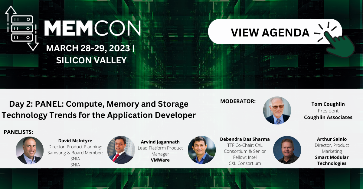
Summit topics include Memory’s Headed for Change, High Performance Data Analytics, CXL 3.0, Detecting Ransomware, Meeting Scaling Challenges, Open Standards for Innovation at the Package Level, and Standardizing Memory to Memory Data Movement. Great panel discussions are on tap as well.  Kurt Lender of the CXL Consortium will lead a discussion on Exploring the CXL Device Ecosystem and Usage Models, Dave Eggleston of Microchip will lead a panel with Samsung and SMART Modular on Persistent Memory Trends, and Cameron Brett of KIOXIA will lead a SSD Form Factors Update.   More details at www.snia.org/cms-summit. Later in 2023… Opportunities for networking will continue throughout 2023. We look forward to seeing you at the SmartNIC Summit (June 13-15), Flash Memory Summit (August 8-10), SNIA Storage Developer Conference (September 18-21), OCP Global Summit (October 17-19), and SC23 (November 12-17). Details on SNIA participation coming soon! The post “Year of the Summit” Kicks Off with Live and Virtual Events first appeared on SNIA Compute, Memory and Storage Blog.

Olivia Rhye

Product Manager, SNIA

Leave a Reply

Comments

Name

Email Adress

Website

Save my name, email, and website in this browser for the next time I comment.

Is EDSFF Taking Center Stage? We Answer Your Questions!

SNIA CMS Community

Jan 11, 2023

title of post
Enterprise and Data Center Form Factor (EDSFF) technologies have come a long way since our 2020 SNIA CMSI webinar on the topic. While that webinar still provides an outstanding framework for understanding – and SNIA’s popular SSD Form Factors page gives the latest on the E1 and E3 specifications – SNIA Solid State Drive Special Interest Group co-chairs Cameron Brett and Jonmichael Hands joined to provide the latest updates at our live webcast: EDSFF Taking Center Stage in the Data Center.  We had some great questions from our live audience, so our experts have taken the time to answer them in this this blog. Q: What does the EDSFF roadmap look like? When will we see PCIe® Gen5 NVMe™, 1.2, 2.0 CXL ™ cx devices? As the form factors come out into the market, we anticipate that there will be feature updates and smaller additions to the existing specifications like SFF TA 1008 and SFF TA 1023.  There may also be changes around defining LEDs and stack updates.  The EDSFF specifications, however, are mature and we have seen validation and support on the connector and how it works at higher interface speeds. You now have platforms, backplanes, and chassis to support these form factors in the marketplace.  Going forward, we may see integration with other device types like GPUs, support of new platforms, and alignment with PCIe Gen 5.  Regarding CXL, we see the buzz, and having this form factor be the kind of vehicle for CXL will have a huge momentum. Q:  I’m looking for thoughts on recent comments I read about PCIe5 NVMe drives likely needing/benefitting from larger form-factors (like 25mm wide vs 22) for cooling considerations. With mass market price optimizations, what is the likelihood that client compute will need to transition away from existing M.2 (esp 2280) form factors in the coming years and will that be a shared form-factor shared with server compute (as has been the case with 5.25″,3.5″,2.5″ drives)? We are big fans of EDSFF being placed on reference platforms for OEMs and motherboard makers. Enterprise storage support would be advantageous on the desktop.  At the recent OCP Global Summit, there was discussion on Gen 5specifications and M.2 and U.2. With the increased demands for power and bandwidth, we think if you want more performance you will need to move to a different form factor, and EDSFF makes sense. Q:  On E1.S vs E3.S market dominance, can you refer to their support on dual-port modules? Some traditional storage server designs favor E3.S because of the dual port configuration. More modern storage designs do not rely on dual port modules, and therefore prefer E1.S. Do you agree to this correlation ? How will this affect the predictions on market share? A:  There is some confusion about the specification support versus what vendors support and what customers are demanding.  The EDSFF specifications share a common pin out and connection specifications.  If a manufacturer wishes to support the dual port functionality, they can do so now. Hyperscalers are now using E1.S in compute designs and may use E3 for their high availability enterprise storage requirements.  Our webcast showed the forecast from Forward Insights on larger shipments of E3 further out in time, reflecting the transition away from 2.5-inch to E3 as server and storage OEMs transition their backplanes. Q:  Have you investigated enabling conduction cooling of E1.S and E3.S to a water cooled cold plate? If not, is it of interest? OCP Global Summit featured a presentation from Intel about immersion cooling with a focus on the sustainability aspect as you can get your power usage effectiveness (PUE) down further by eliminating the fans in system design while increasing cooling. There doesn’t seem to be anything eliminating the use of EDSFF drives for immersion cooling. New CPUs have heat pipes, and new OEM designs have up to 36 drives in a 2U chassis.  How do you cool that?  Many folks are talking about cooling in the data center, and we’ll just need to wait to see what happens! Thanks again for your interest in SNIA and Enterprise and Data Center SSD Form Factors.  We invite you to visit our SSD Form Factor page where we have videos, white papers, and charts explaining the many different SSD sizes and formats in a variety of form factors. The post Is EDSFF Taking Center Stage? We Answer Your Questions! first appeared on SNIA Compute, Memory and Storage Blog.

Olivia Rhye

Product Manager, SNIA

Find a similar article by tags

Leave a Reply

Comments

Name

Email Adress

Website

Save my name, email, and website in this browser for the next time I comment.

Is the Data Really Gone? A Q&A

SNIA CMSI

Aug 25, 2022

title of post

In our recent webcast Is the Data Really Gone? A Primer on the Sanitization of Storage Devices, our presenters Jonmichael Hands (Chia Network), Jim Hatfield (Seagate), and John Geldman (KIOXIA) took an in-depth look at exactly what sanitization is, what the standards are, and where sanitization is being practiced today.  If you missed it, you can watch on-demand their recommendations for the verification of sanitization to ensure that devices are meeting stringent requirements – and access the presentation slides at the SNIA Educational Library.  Here, in our Q&A blog, our experts answer more of your questions on data sanitization.

Is Over Provisioning part of the spare blocks or separate?

The main intent of an overprovisioning strategy is to resolve the asymmetric NAND behaviors of Block Erase (e.g., MBs) and Page Write (e.g., KBs) that allows efficient use of a NAND die’s endurance capability, in other words, it is a store-over capability that is regularly used leaving older versions of a Logical Block Addressing (LBA) in media until it is appropriate to garbage collect.

Spares are a subset of overprovisioning and a spare block strategy is different than an overprovisioning strategy. The main intent of a spare strategy is a failover capability mainly used on some kind of failure (this can be a temporary vibration issue on a hard disk drive or a bad sector).

The National Institute of Standards and Technology (NIST) mentions the NVMe® Format with Secure Erase Settings to 1 for User Data erase or 2 for Crypto as a purge method. From what I can gather the sanitize was more a fallout of the format rather than anything that was designed. With the NVMe sanitize would you expect the Format with the Data Erasure options to be depreciated or moved back to a clear?

The Format NVM command does have a crypto erase, but it is entirely unspecified, vendor specific, and without any requirements. It is not to be trusted. Sanitize, however, can be trusted, has specific TESTABLE requirements, and is sanctioned by IEEE 2883.

The Format NVM command was silent on some requirements that are explicit in both NVMe Sanitize commands and IEEE 2883. It was possible, but not required for a NVME Format with Secure Erase Settings set to Crypto to also purge other internal buffers. Such behavior beyond the specification is vendor specific. Without assurance from the vendor, be wary of assuming the vendor made additional design efforts. The NVMe Sanitize command does meet the requirements of purge as defined in IEEE 2883.

My question is around logical (file-level, OS/Filesystem, Logical volumes, not able to apply to physical DDMs): What can be done at the technical level and to what degree that it is beyond what modern arrays can do (e.g., too many logical layers) and thus, that falls under procedural controls. Can you comment on regulatory alignment with technical (or procedural) acceptable practices?

The IEEE Security in Storage Working Group (SISWG) has not had participation by subject matter experts for this, and therefore has not made any requirements or recommendations, and acceptable practices. Should such experts participate, we can consider requirements and recommendations and acceptable practices.

Full verification is very expensive especially if you are doing lots of drives simultaneously. Why can't you seed like you could do for crypto, verify the seeding is gone, and then do representative sampling?

The problem with seeding before crypto erase is that you don’t know the before and after data to actually compare with. Reading after crypto erase returns garbage…. but you don’t know if it is the right garbage.  In addition, in some implementations, doing a crypto erase also destroys the CRC/EDC/ECC information making the data unreadable after crypto erase.

Seeding is not a common defined term. If what was intended by seeding was writing known values into known locations, be aware that there are multiple problems with that process. Consider an Overwrite Sanitize operation. Such an operation writes the same pattern into every accessible and non-accessible block. That means that the device is completely written with no free media (even the overprovisioning has that pattern). For SSDs, a new write into that device has to erase data before it can be re-written. This lack of overprovisioned data in SSDs results in artificial accelerated endurance issues.

A common solution implemented by multiple companies is to de-allocate after sanitization. After a de-allocation, a logical block address will not access physical media until that logical block address is written by the host. This means that even if known data was written before sanitize, and if the sanitize did not do its job, then the read-back will not return the data from the physical media that used to be allocated to that address (i.e., that physical block is de-allocated) so the intended test will not be effective.

Are there other problems with Sanitize?

Another problem with Sanitize is that internal protection information (e.g., CRC data, Integrity Check data, and Error Correction Code data) have also been neutralized until that block is written again with new data. Most SSDs are designed to never return bad data (e.g., data that fails Integrity Checks) as a protection and reliability feature.

What are some solutions for Data Sanitization?

One solution that has been designed into NVMe is for the vendor to support a full overwrite of media after a crypto erase or a block erase sanitize operation. Note that such an overwrite has unpopular side-effects as the overwrite:

  1. changes any result of the actual sanitize operation;
  2. may take a significant time (e.g., multiple days); and
  3. still requires a full-deallocation by the host to make the device useful again.

A unique complication for a Block Erase sanitization operation that leaves NAND in an erased state is not stable at the NAND layer, so a full write of deallocated media can be scheduled to be done over time, or the device can be designed to complete an overwrite before the sanitize operation returns a completion. In any/either case, the media remains deallocated until the blocks are written by the host.

Can you kindly clarify DEALLOCATE all storage before leaving sanitize ? What does that mean physically?

Deallocation (by itself) is not acceptable for sanitization. It is allowable AFTER a proper and thorough sanitization has taken place. Also, in some implementations, reading a deallocated logical block results in a read error. Deallocation must be USED WITH CAUTION. There are many knobs and switches to set to do it right.

Deallocation means removing the internal addressing that mapped a logical block to a physical block. After deallocation, media is not accessed so the read of a logical block address provides no help in determining if the media was actually sanitized or not. Deallocation gives as factory-fresh out of the box performance as is possible.

Olivia Rhye

Product Manager, SNIA

Find a similar article by tags

Leave a Reply

Comments

Name

Email Adress

Website

Save my name, email, and website in this browser for the next time I comment.

Is the Data Really Gone? A Q&A

SNIA CMS Community

Aug 25, 2022

title of post
In our recent webcast Is the Data Really Gone? A Primer on the Sanitization of Storage Devices, our presenters Jonmichael Hands (Chia Network), Jim Hatfield (Seagate), and John Geldman (KIOXIA) took an in-depth look at exactly what sanitization is, what the standards are, and where sanitization is being practiced today.  If you missed it, you can watch on-demand their recommendations for the verification of sanitization to ensure that devices are meeting stringent requirements – and access the presentation slides at the SNIA Educational Library.  Here, in our Q&A blog, our experts answer more of your questions on data sanitization. Is Over Provisioning part of the spare blocks or separate? The main intent of an overprovisioning strategy is to resolve the asymmetric NAND behaviors of Block Erase (e.g., MBs) and Page Write (e.g., KBs) that allows efficient use of a NAND die’s endurance capability, in other words, it is a store-over capability that is regularly used leaving older versions of a Logical Block Addressing (LBA) in media until it is appropriate to garbage collect. Spares are a subset of overprovisioning and a spare block strategy is different than an overprovisioning strategy. The main intent of a spare strategy is a failover capability mainly used on some kind of failure (this can be a temporary vibration issue on a hard disk drive or a bad sector). The National Institute of Standards and Technology (NIST) mentions the NVMe® Format with Secure Erase Settings to 1 for User Data erase or 2 for Crypto as a purge method. From what I can gather the sanitize was more a fallout of the format rather than anything that was designed. With the NVMe sanitize would you expect the Format with the Data Erasure options to be depreciated or moved back to a clear? The Format NVM command does have a crypto erase, but it is entirely unspecified, vendor specific, and without any requirements. It is not to be trusted. Sanitize, however, can be trusted, has specific TESTABLE requirements, and is sanctioned by IEEE 2883. The Format NVM command was silent on some requirements that are explicit in both NVMe Sanitize commands and IEEE 2883. It was possible, but not required for a NVME Format with Secure Erase Settings set to Crypto to also purge other internal buffers. Such behavior beyond the specification is vendor specific. Without assurance from the vendor, be wary of assuming the vendor made additional design efforts. The NVMe Sanitize command does meet the requirements of purge as defined in IEEE 2883. My question is around logical (file-level, OS/Filesystem, Logical volumes, not able to apply to physical DDMs): What can be done at the technical level and to what degree that it is beyond what modern arrays can do (e.g., too many logical layers) and thus, that falls under procedural controls. Can you comment on regulatory alignment with technical (or procedural) acceptable practices? The IEEE Security in Storage Working Group (SISWG) has not had participation by subject matter experts for this, and therefore has not made any requirements or recommendations, and acceptable practices. Should such experts participate, we can consider requirements and recommendations and acceptable practices. Full verification is very expensive especially if you are doing lots of drives simultaneously. Why can’t you seed like you could do for crypto, verify the seeding is gone, and then do representative sampling? The problem with seeding before crypto erase is that you don’t know the before and after data to actually compare with. Reading after crypto erase returns garbage…. but you don’t know if it is the right garbage. In addition, in some implementations, doing a crypto erase also destroys the CRC/EDC/ECC information making the data unreadable after crypto erase. Seeding is not a common defined term. If what was intended by seeding was writing known values into known locations, be aware that there are multiple problems with that process. Consider an Overwrite Sanitize operation. Such an operation writes the same pattern into every accessible and non-accessible block. That means that the device is completely written with no free media (even the overprovisioning has that pattern). For SSDs, a new write into that device has to erase data before it can be re-written. This lack of overprovisioned data in SSDs results in artificial accelerated endurance issues. A common solution implemented by multiple companies is to de-allocate after sanitization. After a de-allocation, a logical block address will not access physical media until that logical block address is written by the host. This means that even if known data was written before sanitize, and if the sanitize did not do its job, then the read-back will not return the data from the physical media that used to be allocated to that address (i.e., that physical block is de-allocated) so the intended test will not be effective. Are there other problems with Sanitize? Another problem with Sanitize is that internal protection information (e.g., CRC data, Integrity Check data, and Error Correction Code data) have also been neutralized until that block is written again with new data. Most SSDs are designed to never return bad data (e.g., data that fails Integrity Checks) as a protection and reliability feature. What are some solutions for Data Sanitization? One solution that has been designed into NVMe is for the vendor to support a full overwrite of media after a crypto erase or a block erase sanitize operation. Note that such an overwrite has unpopular side-effects as the overwrite:
  1. changes any result of the actual sanitize operation;
  2. may take a significant time (e.g., multiple days); and
  3. still requires a full-deallocation by the host to make the device useful again.
A unique complication for a Block Erase sanitization operation that leaves NAND in an erased state is not stable at the NAND layer, so a full write of deallocated media can be scheduled to be done over time, or the device can be designed to complete an overwrite before the sanitize operation returns a completion. In any/either case, the media remains deallocated until the blocks are written by the host. Can you kindly clarify DEALLOCATE all storage before leaving sanitize ? What does that mean physically? Deallocation (by itself) is not acceptable for sanitization. It is allowable AFTER a proper and thorough sanitization has taken place. Also, in some implementations, reading a deallocated logical block results in a read error. Deallocation must be USED WITH CAUTION. There are many knobs and switches to set to do it right. Deallocation means removing the internal addressing that mapped a logical block to a physical block. After deallocation, media is not accessed so the read of a logical block address provides no help in determining if the media was actually sanitized or not. Deallocation gives as factory-fresh out of the box performance as is possible. The post Is the Data Really Gone? A Q&A first appeared on SNIA Compute, Memory and Storage Blog.

Olivia Rhye

Product Manager, SNIA

Find a similar article by tags

Leave a Reply

Comments

Name

Email Adress

Website

Save my name, email, and website in this browser for the next time I comment.

Join Us as We Return Live to FMS!

SNIA CMS Community

Jul 29, 2022

title of post
SNIA is pleased to be part of the Flash Memory Summit 2022 agenda August 1-4, 2022 at the Santa Clara CA Convention Center, with our volunteer leadership demonstrating solutions, chairing and speaking in sessions, and networking with FMS attendees at a variety of venues during the conference. The ever-popular SNIA Reception at FMS features the SNIA groups Storage Management Initiative, Compute Memory and Storage Initiative, and Green Storage Initiative, along with SNIA alliance partners CXL Consortium, NVM Express, and OpenFabrics Alliance.  Stop by B-203/204 at the Convention Center from 5:30 – 7:00 pm Monday August 1 for refreshments and networking with colleagues to kick off the week! You won’t want to miss SNIA’s mainstage presentation on Wednesday August 3 at 2:40 pm in the Mission City Ballroom. SNIA Vice Chair Richelle Ahlvers of Intel will provide a perspective on how new storage technologies and trends are accelerating through standards and open communities. In the Exhibit Hall, SNIA Storage Management Initiative and Compute Memory and Storage Initiative are FMS Platinum sponsors with a SNIA Demonstration Pavilion at booth #725.  During exhibit hours Tuesday evening through Thursday afternoon, 15 SNIA member companies will be featured in live technology demonstrations on storage management, computational storage, persistent memory, sustainability, and form factors; a Persistent Memory Programming Workshop and Hackathon; and theater presentations on SNIA’s standards and alliance work. Long standing SNIA technology focus areas in computational storage and memory will be represented in the SNIA sponsored System Architectures Track (SARC for short) – Tuesday for memory and Thursday for computational storage.  SNIA is also pleased to sponsor a day on CXL architectures, memory, and storage talks on Wednesday. These sessions will all be in Ballroom G. A new Sustainability Track on Thursday morning in Ballroom A led by the SNIA Green Storage Technical Work Group includes presentations on SSD power management, real world applications and storage workloads, and a carbon footprint comparison of SSDs vis HDDs, followed by a panel discussion. SSDs will also be featured in two SNIA-led presentation/panel pairs – SSDS-102-1 and 102-2 Ethernet SSDs on Tuesday afternoon in Ballroom B and SSDS-201-1 and 201-2 EDSFF E1 and E3 form factors on Wednesday morning in Ballroom D. SNIA Swordfish will be discussed in the DCTR-102-2 Enterprise Storage Part 2 session in Ballroom D on Tuesday morning And the newest SNIA technical work group – DNA Data Storage– will lead a new-to-2022 FMS track on Thursday morning in Great America Meeting Room 2, discussing topics like preservation of DNA for information storage, the looming need for molecular storage, and DNA sequencing at scale. Attendees can engage for questions and discussion in Part 2 of the track. Additional ways to network with SNIA colleagues include the always popular chat with the experts – beer and pizza on Tuesday evening, sessions on cloud storage, artificial intelligence, blockchain, and an FMS theater presentation on real world storage workloads. Full details on session times, locations, chairs and speakers for all these exciting FMS activities can be found at www.snia.org/fms and on the Flash Memory Summit website.  SNIA colleagues and friends can register for $100.00 off the full conference or single day packages using the code SNIA22 at www.flashmemorysummit.com. The post Join Us as We Return Live to FMS! first appeared on SNIA Compute, Memory and Storage Blog.

Olivia Rhye

Product Manager, SNIA

Leave a Reply

Comments

Name

Email Adress

Website

Save my name, email, and website in this browser for the next time I comment.

See You – Virtually – at SDC 2021

Marty Foltyn

Sep 23, 2021

title of post
SNIA Storage Developer Conference goes virtual September 28-29 2021, and compute, memory, and storage are important topics.  SNIA Compute, Memory, and Storage Initiative is a sponsor of SDC 2021 – so visit our booth for the latest information and a chance to chat with our experts.  With over 120 sessions available to watch live during the event and later on-demand, live Birds of a Feather chats, and a Persistent Memory Bootcamp and Hackathon accessing new systems in the cloud, we want to make sure you don’t miss anything!  Register here to see sessions live – or on demand to your schedule. Agenda highlights include: LIVE Birds of a Feather Sessions are OPEN to all – SDC registration not required. Here is your chance, via zoom, to ask your questions of the SNIA experts.  Registration links will go live on September 28 and 29 at this page link. Computational Storage Talks A great video provides an overview of sessions. Watch it here.
  • Computational Storage APIs – how the SNIA Computational Storage TWG is leading the way with new interface definitions with Computational Storage APIs that work across different hardware architectures.
  • NVMe Computational Storage Update – Learn what is happening in NVMe to support Computational Storage devices, including a high level architecture that is being defined in NVMe for Computational Storage. The architecture provides for programs based on a standardized eBPF. (Check out our blog on eBPF.)
Persistent Memory Presentations A great video provides an overview of sessions. Watch it here. The post See You – Virtually – at SDC 2021 first appeared on SNIA Compute, Memory and Storage Blog.

Olivia Rhye

Product Manager, SNIA

Leave a Reply

Comments

Name

Email Adress

Website

Save my name, email, and website in this browser for the next time I comment.

NVMe Key-Value Standard Q&A

John Kim

Nov 9, 2020

title of post

Last month, Bill Martin, SNIA Technical Council Co-Chair, presented a detailed update on what’s happening in the development and deployment of the NVMe Key-Value standard. Bill explained where Key Value fits within an architecture, why it’s important, and the standards work that is being done between NVM Express and SNIA. The webcast was one of our highest rated. If you missed it, it’s available on-demand along with the webcast slides. Attendees at the live event had many great questions, which Bill Martin has answered here:

Q. Two of the most common KV storage mechanisms in use today are AWS S3 and RocksDB. How does NVMe KV standards align or differ from them? How difficult would it be to map between the APIs and semantics of those other technologies to NVMe KV devices?

A. KV Storage is intended as a storage layer that would support these and other object storage mechanisms. There is a publicly available KVRocks: RocksDB compatible key value store and MyRocks compatible storage engine designed for KV SSDs at GitHub. There is also a Ceph Object storage design available. These are example implementations that can help an implementer get to an efficient use of NVMe KV storage.

Q. At which layer will my app stack need to change to take advantage of KV storage?  Will VMware or Linux or Windows need to change at the driver level?  Or do the apps need to be changed to treat data differently?  If the apps don’t need to change doesn’t this then just take the data layout tables and move them up the stack in to the server?

A. The application stack needs to change at the point where it interfaces to a filesystem, where the interface would change from a filesystem interface to a KV storage interface. In order to take advantage of Key Value storage, the application itself may need to change, depending on what the current application interface is. If the application is talking to a RocksDB or similar interface, then the driver could simply be changed out to allow the app to talk directly to Key Value Storage. In this case, the application does not care about the API or the underlying storage. If the application is currently interfacing to a filesystem, then the application itself would indeed need to change and the KV API provides a standardized interface that multiple vendors can support to provide both the necessary libraries and access to a Key Value storage device. There will need to be changes in the OS to support this in providing a kernel layer driver for the NVMe KV device. If the application is using an existing driver stack that goes through a filesystem and does not change, then you cannot take advantage of KV Storage, but if the application changes or already has an object storage interface then the kernel filesystem and mapping functions can be removed from the data path.

Q. Is there a limit to the length of a key or value in the KV Architecture?

A.There are limits to the Key and value sizes in the current NVMe standard. The current implementation limits the key to 16 bytes due to a desire to pass the key within the NVMe command. The other architectural limit on a key is that the length of the key is specified in a field that allows up to 255 bytes for the key length. To utilize this, an alternative mechanism for passing the key to the device is necessary. For the value, the limit on the size is 4 GBytes.

Q. Are there any atomicity guarantees (e.g. for overwrites)?

A. The current specification makes it mandatory for atomicity at the KV level. In other words, if a KV Store command overwrites an existing KV pair and there is a power failure, you either get all of the original value or all of the new value.

Q. Is KV storage for a special class of storage called computational storage or can it be used for general purpose storage?

A. This is for any application that benefits from storing objects as opposed to storing blocks. This is unrelated to computational storage but may be of use in computational storage applications. One application that has been considered is that for a filesystem that rather than using the filesystem for storing blocks and having a mapping of each file handle to a set of blocks that contain the file contents, you would use KV storage where the file handle is the key and the object holds the file contents.

Q. What are the most frequently used devices to use the KV structure?

A. If what is being asked is, what are the devices that provide a KV structure, then the answer is, we expect the most common devices using the KV structure will be KV SSDs.

Q. Does the NVMe KV interface require 2 accessed in order to get the value (i.e., on access to get the value size in order to allocate the buffer and then a second access to read the value)?

A.If you know the size of the object or if you can pre-allocate enough space for your maximum size object then you can do a single access. This is no different than current implementations where you actually have to specify how much data you are retrieving from the storage device by specifying a starting LBA and a length. If you do not know the size of the value and require that in order to retrieve the value then you would indeed need to submit two commands to the NVMe KV storage device.

Q. Does the device know whether an object was compressed, and if not how can a previously compressed object be stored?

A. The hardware knows if it does compression automatically and therefore whether it should de-compress the object. If the storage device supports compression and the no-compress option, then the device will store metadata with the KV pair indicating if no-compress was specified when storing the file in order to return appropriate data. If the KV storage device does not perform compression, it can simply support storage and retrieval of previously compressed objects. If the KV storage device performs its own compression and is given a previously-compressed object to store and the no-compress option is not requested, the device will recompress the value (which typically won’t result in any space savings) or if the no-compress option is requested the device will store the value without attempting additional compression.

Q. On flash, erased blocks are fixed sizes, so how does Key Value handle defrag after a lot of writes and deletes?

A. This is implementation specific and depends on the size of the values that are stored. This is much more efficient on values that are approximately the size of the device’s erase block size as those values may be stored in an erase block and when deleted the erase block can be erased. For smaller values, an implementation would need to manage garbage collection as values are deleted and when appropriate move values that remain in a mostly empty erase block into a new erase block prior to erasing the erase block. This is no different than current garbage collection. The NVMe KV standard provides a mechanism for the device to report optimal value size to the host in order to better manage this as well.

Q. What about encryption?  Supported now or will there be SED versions of [key value] drives released down the road?

A. There is no reason that a product could not support encryption with the current definition of key value storage. The release of SED (self-encrypting drive) products is vendor specific.

Q. What are considered to be best use cases for this technology? And for those use cases - what's the expected performance improvement vs. current NVMe drives + software?

A. The initial use case is for database applications where the database is already storing key/value pairs. In this use case, experimentation has shown that a 6x performance improvement from RocksDB to a KV SSD implementing KV-Rocks is possible.

Q. Since writes are complete (value must be written altogether), does this mean values are restricted to NVMe's MDTS?

 A. Yes. Values are limited by MDTS (maximum data transfer size). A KV device may set this value to something greater than a block storage device does in order to support larger value sizes.

Q. How do protection scheme works with key-value (erasure coding/RAID/...)?

A. Since key value deals with complete values as opposed to blocks that make up a user data, RAID and erasure coding are usually not applicable to key value systems. The most appropriate data protection scheme for key value storage devices would be a mirrored scheme. If a storage solution performed erasure coding on data first, it could store the resulting EC fragments or symbols on key value SSDs.

Q. So Key Value is not something built on top of block like Object and NFS are?  Object and NFS data are still stored on disks that operate on sectors, so object and NFS are layers on top of block storage?  KV is drastically different, uses different drive firmware and drive layout?  Or do the drives still work the same and KV is another way of storing data on them alongside block, object, NFS?

A. Today, there is only one storage paradigm at the drive level -- block. Object and NFS are mechanisms in the host to map data models onto block storage. Key Value storage is a mechanism for the storage device to map from an address (a key) to a physical location where the value is stored, avoiding a translation in the host from the Key/value pair to a set of block addresses which are then mapped to physical locations where data is then stored. A device may have one namespace that stores blocks and another namespace that stores key value pairs. There is not a difference in the low-level storage mechanism only in the mapping process from address to physical location. Another difference from block storage is that the value stored is not a fixed size.

Q. Could you explain more about how tx/s is increased with KV?

A. The increase in transfers/second occurs for two reasons: one is because the translation layer in the host from key/value to block storage is removed; the second is that the commands over the bus are reduced to a single transfer for the entire key value pair. The latency savings from this second reduction is less significant than the savings from removing translation operations that have to happen in the host.

Keep up-to-date on work SNIA is doing on the Key Value Storage API Specification at the SNIA website.

Olivia Rhye

Product Manager, SNIA

Find a similar article by tags

Leave a Reply

Comments

Name

Email Adress

Website

Save my name, email, and website in this browser for the next time I comment.

NVMe Key-Value Standard Q&A

John Kim

Nov 9, 2020

title of post
Last month, Bill Martin, SNIA Technical Council Co-Chair, presented a detailed update on what’s happening in the development and deployment of the NVMe Key-Value standard. Bill explained where Key Value fits within an architecture, why it’s important, and the standards work that is being done between NVM Express and SNIA. The webcast was one of our highest rated. If you missed it, it’s available on-demand along with the webcast slides. Attendees at the live event had many great questions, which Bill Martin has answered here: Q. Two of the most common KV storage mechanisms in use today are AWS S3 and RocksDB. How does NVMe KV standards align or differ from them? How difficult would it be to map between the APIs and semantics of those other technologies to NVMe KV devices? A. KV Storage is intended as a storage layer that would support these and other object storage mechanisms. There is a publicly available KVRocks: RocksDB compatible key value store and MyRocks compatible storage engine designed for KV SSDs at GitHub. There is also a Ceph Object storage design available. These are example implementations that can help an implementer get to an efficient use of NVMe KV storage. Q. At which layer will my app stack need to change to take advantage of KV storage?  Will VMware or Linux or Windows need to change at the driver level?  Or do the apps need to be changed to treat data differently?  If the apps don’t need to change doesn’t this then just take the data layout tables and move them up the stack in to the server? A. The application stack needs to change at the point where it interfaces to a filesystem, where the interface would change from a filesystem interface to a KV storage interface. In order to take advantage of Key Value storage, the application itself may need to change, depending on what the current application interface is. If the application is talking to a RocksDB or similar interface, then the driver could simply be changed out to allow the app to talk directly to Key Value Storage. In this case, the application does not care about the API or the underlying storage. If the application is currently interfacing to a filesystem, then the application itself would indeed need to change and the KV API provides a standardized interface that multiple vendors can support to provide both the necessary libraries and access to a Key Value storage device. There will need to be changes in the OS to support this in providing a kernel layer driver for the NVMe KV device. If the application is using an existing driver stack that goes through a filesystem and does not change, then you cannot take advantage of KV Storage, but if the application changes or already has an object storage interface then the kernel filesystem and mapping functions can be removed from the data path. Q. Is there a limit to the length of a key or value in the KV Architecture? A.There are limits to the Key and value sizes in the current NVMe standard. The current implementation limits the key to 16 bytes due to a desire to pass the key within the NVMe command. The other architectural limit on a key is that the length of the key is specified in a field that allows up to 255 bytes for the key length. To utilize this, an alternative mechanism for passing the key to the device is necessary. For the value, the limit on the size is 4 GBytes. Q. Are there any atomicity guarantees (e.g. for overwrites)? A. The current specification makes it mandatory for atomicity at the KV level. In other words, if a KV Store command overwrites an existing KV pair and there is a power failure, you either get all of the original value or all of the new value. Q. Is KV storage for a special class of storage called computational storage or can it be used for general purpose storage? A. This is for any application that benefits from storing objects as opposed to storing blocks. This is unrelated to computational storage but may be of use in computational storage applications. One application that has been considered is that for a filesystem that rather than using the filesystem for storing blocks and having a mapping of each file handle to a set of blocks that contain the file contents, you would use KV storage where the file handle is the key and the object holds the file contents. Q. What are the most frequently used devices to use the KV structure? A. If what is being asked is, what are the devices that provide a KV structure, then the answer is, we expect the most common devices using the KV structure will be KV SSDs. Q. Does the NVMe KV interface require 2 accessed in order to get the value (i.e., on access to get the value size in order to allocate the buffer and then a second access to read the value)? A.If you know the size of the object or if you can pre-allocate enough space for your maximum size object then you can do a single access. This is no different than current implementations where you actually have to specify how much data you are retrieving from the storage device by specifying a starting LBA and a length. If you do not know the size of the value and require that in order to retrieve the value then you would indeed need to submit two commands to the NVMe KV storage device. Q. Does the device know whether an object was compressed, and if not how can a previously compressed object be stored? A. The hardware knows if it does compression automatically and therefore whether it should de-compress the object. If the storage device supports compression and the no-compress option, then the device will store metadata with the KV pair indicating if no-compress was specified when storing the file in order to return appropriate data. If the KV storage device does not perform compression, it can simply support storage and retrieval of previously compressed objects. If the KV storage device performs its own compression and is given a previously-compressed object to store and the no-compress option is not requested, the device will recompress the value (which typically won’t result in any space savings) or if the no-compress option is requested the device will store the value without attempting additional compression. Q. On flash, erased blocks are fixed sizes, so how does Key Value handle defrag after a lot of writes and deletes? A. This is implementation specific and depends on the size of the values that are stored. This is much more efficient on values that are approximately the size of the device’s erase block size as those values may be stored in an erase block and when deleted the erase block can be erased. For smaller values, an implementation would need to manage garbage collection as values are deleted and when appropriate move values that remain in a mostly empty erase block into a new erase block prior to erasing the erase block. This is no different than current garbage collection. The NVMe KV standard provides a mechanism for the device to report optimal value size to the host in order to better manage this as well. Q. What about encryption?  Supported now or will there be SED versions of [key value] drives released down the road? A. There is no reason that a product could not support encryption with the current definition of key value storage. The release of SED (self-encrypting drive) products is vendor specific. Q. What are considered to be best use cases for this technology? And for those use cases – what’s the expected performance improvement vs. current NVMe drives + software? A. The initial use case is for database applications where the database is already storing key/value pairs. In this use case, experimentation has shown that a 6x performance improvement from RocksDB to a KV SSD implementing KV-Rocks is possible. Q. Since writes are complete (value must be written altogether), does this mean values are restricted to NVMe’s MDTS? A. Yes. Values are limited by MDTS (maximum data transfer size). A KV device may set this value to something greater than a block storage device does in order to support larger value sizes. Q. How do protection scheme works with key-value (erasure coding/RAID/…)? A. Since key value deals with complete values as opposed to blocks that make up a user data, RAID and erasure coding are usually not applicable to key value systems. The most appropriate data protection scheme for key value storage devices would be a mirrored scheme. If a storage solution performed erasure coding on data first, it could store the resulting EC fragments or symbols on key value SSDs. Q. So Key Value is not something built on top of block like Object and NFS are?  Object and NFS data are still stored on disks that operate on sectors, so object and NFS are layers on top of block storage?  KV is drastically different, uses different drive firmware and drive layout?  Or do the drives still work the same and KV is another way of storing data on them alongside block, object, NFS? A. Today, there is only one storage paradigm at the drive level — block. Object and NFS are mechanisms in the host to map data models onto block storage. Key Value storage is a mechanism for the storage device to map from an address (a key) to a physical location where the value is stored, avoiding a translation in the host from the Key/value pair to a set of block addresses which are then mapped to physical locations where data is then stored. A device may have one namespace that stores blocks and another namespace that stores key value pairs. There is not a difference in the low-level storage mechanism only in the mapping process from address to physical location. Another difference from block storage is that the value stored is not a fixed size. Q. Could you explain more about how tx/s is increased with KV? A. The increase in transfers/second occurs for two reasons: one is because the translation layer in the host from key/value to block storage is removed; the second is that the commands over the bus are reduced to a single transfer for the entire key value pair. The latency savings from this second reduction is less significant than the savings from removing translation operations that have to happen in the host. Keep up-to-date on work SNIA is doing on the Key Value Storage API Specification at the SNIA website.

Olivia Rhye

Product Manager, SNIA

Leave a Reply

Comments

Name

Email Adress

Website

Save my name, email, and website in this browser for the next time I comment.

Answering Your Questions on EDSFF

Jonmichael Hands

Oct 19, 2020

title of post
We had a tremendous response to our webcast asking if we were truly at the end of the 2.5-inch disk era. SNIA Compute, Memory, and Storage Initiative SSD Special Interest Group brought together experts from Dell, Facebook, HPE, JEDEC, KIOXIA, Lenovo, and Microsoft in a lively follow on to the Enterprise and Data Center SSD Form Factor (EDSFF) May 2020 discussions at OCP Summit,. If you missed our live webcast – watch it on demand. Webcast attendees raised a variety of questions.  Our experts provide answers to them here: Q:  SFF_TA_1006 suggests E1.S can support max 25W for 25mm asymmetric heat-sink. What are the air-flow assumptions for this estimate? Are there any thermal models and test guidelines available for EDSFF form-factors? A:  Yes! The SNIA SFF TA TWG has a new project on Enterprise Device Form Factor Thermal Requirements. There was a great presentation about this at the OCP 2020 Virtual Summit. Registered attendees can log in to view. Q:  When is the transition form U.2 to E3 expected to occur? A:  We expect a few products for PCIe 4.0 but a wide industry transition at PCIe 5.0 Q:  No one is mentioning dual-path.  Is this an Enterprise requirement and does EDSFF connector support this? A:  EDSFF does support dual port and enterprise storage high availability applications, with a dual port enable pin, if the SSD vendor supports it. Q:  What is the future vision as to fault tolerance options (RAID, mirroring, etc) for these devices in data center use cases in a way that doesn’t compromise or bottleneck their performance? HW raid controllers could bottleneck on PCIe bandwidth as one speaker mentioned, and SW RAID or virtual SAN solution overhead + application workloads could bottleneck on CPU before you’re able to max out storage performance (especially at these extreme density possibilities, wow!). Thanks! A:  SNIA just did a webcast on NVMe RAID!! See it in our Educational Library: RAID on CPU RAID for NVMe SSDs without a RAID Controller Card Q:  For open frame drives, is a Bezel required for EMI containment? A:  Yes, a latch is expected to have some EMI design Q:  Do all EDSFF form-factors support hot-plugging? Can EDSFF physical form-factors support all capabilities defined in NVMe (storage) specification? A:  Yes, hot plug is expected on EDSFF drives and is included in the SFF-TA-1009 pinout spec for support (interface and presence detect pins). Q:  Can a 2U system plug 2xE1.S into the same bay as 1xE3.S can be inserted? A:  This would require a custom PCB or carrier card. A single E1.S is electrically compatible with an E3 slot. Q:  If the ‘1’ in E1.L and E1.S means ‘1 Rack Unit’ what does the ‘3’ in the E3 family means since it is compatible with 1U and 2U? A:  Correct, E3 was originally for “3in media device” intended to be optimal for 2U vertically oriented, or a 1U horizontal. Q:  Can you estimate the shipment volume share for each form factors? Especially I’d like to know 70W E3.L shipment units forecast. A: As an example, Intel has publicly stated that they expect up to 35% of the data center SSD revenue total market to be on EDSFF by 2024. Analysts like Forward Insights have detailed EDSFF and SSD form factor market analysis. Q:  No one is talking about shock and vibe for this connector.  Is this an exercise for the carrier designer? A:  Mechanical specifications are expected to be similar to U.2 drives today. Q:  With the 2.5″ challenges, and migration to other form factors, what about client systems? It would seem the x4 interfaces would work just fine on a desktop, and the slimmest E1.S on a laptop for better heat dissipation. A:  Many people think M.2 will not be adequate for PCIe 5.0 speeds and power, and companies are looking at reusing E1.S or another client EDSFF variant with the same connector as a successor for desktops and workstations. Q:  Is there a detailed standard of SSDs configuration with different device types, and once there is an error, could SSDs be combined to solve the error problem? A:  SSD data protection is generally solved with RAID, software mirroring, or erasure code. Q:  When will volume servers support the new form factors/connectors? A:  We already see production servers for EDSFF from Supermicro, Wiwynn, AIC, and announcements from Lenovo and others launching soon! Q:  Is U.3 dead? A:   U.3 means conforming to the SFF-TA-1001 link definition specification for the SFF-8639 connector.  It isn’t a form factor definition like EDSFF, and it applies to U.2 (2.5” form factor) drives used with a Tri-mode HBA and properly enabled system backplane.  Read more about U.3 with this article. Intel and other suppliers are transitioning from U.2 & M.2 directly to EDSFF, bypassing support for U.3.  Some companies are supporting U.3 technology through servers, HBAs, and SSDs.

Olivia Rhye

Product Manager, SNIA

Leave a Reply

Comments

Name

Email Adress

Website

Save my name, email, and website in this browser for the next time I comment.

Subscribe to Solid State Storage